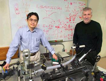
Kin Man Yu and Wladek Walukiewicz have tested the optical and photovoltaic effects of several novel solar cell materials.
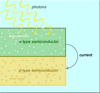
How solar cells work
Sunlight comes in many colors, combining low-energy
infrared photons with high-energy ultraviolet photons and all the visible-light
photons between. Each photovoltaic material responds to a narrow range
of these energies, corresponding to its characteristic band gap.
The band gap is the amount of energy, expressed
in electron volts (eV), required to kick an electron from a semiconductor's
valence band, which is chock full of electrons bound to atoms, into its
empty conduction band, where electrons are free to move. (The bands are
graphical representations, not physical spaces.)
If the semiconductor is doped with impurity atoms
to form an n-type, electrically negative material, it already has a few
electrons in the conduction band; conversely p-type (positive) material
has been doped to leave missing electrons, or holes, in the valence band.
A junction between n- and p-type creates a voltage bias; when incoming
photons are absorbed, electrons migrate toward the positive side of the
junction and holes toward the negative side, forming an electric current.
Discovering the multigap phenomenon
"The concept of multiband cells goes back to solar-cell
pioneer Martin Wolf, who proposed the impurity photovoltaic effect in 1960,"
says Walukiewicz. "The idea was that by introducing impurities with the
right electronic properties into a semiconductor you could make a singlejunction
solar cell that absorbs more photons with different energies. Sounds easy,
but nobody knew how to do it."
But in 1999, Walukiewicz and others at Berkeley
Lab were working with solar-cell designers at DOE's National Renewable
Energy Laboratory, who were trying to build a three-junction cell. The
NREL researchers inadvertently created the first photovoltaic semiconductor
with a split band gap. But at first they didn't realize it.
"They needed a new material with a 1-eV band gap
and a crystal lattice structure that matched the other layers of the cell,"
Walukiewicz explains. ""They used gallium indium arsenide nitride alloys
in which just a little nitrogen could achieve the desired band gapand
an almost perfect lattice match."
Since the band-gap reduction was unexpected, Walukiewicz
set out to find out how it worked. The answer, it developed, was that the
few atoms of nitrogen, which are much more electronegative than the host
atoms (much more strongly attractive to electrons) produced a narrow energy
band of their own, splitting the GaInAs conduction band into two parts.
The gap to the lower of the two conduction bands was the desired 1 eV.
In the case of GaInAs, other characteristics of
the split bands made for a poor solar cell material. Nevertheless, Walukiewicz
and his colleagues continued to investigate the phenomenon and developed
a model of the split-band phenomenon known as "band anticrossing."
A perfect mismatch
A so-called highly mismatched alloy results when
a few of the host atoms of a semiconductor alloy in the III-V group, like
GaInAs, are replaced with nitrogen atoms having very different electronegativity.
(The Roman numerals refer to the columns in the periodic table in which
the constituent elements are found.) Replacing atoms in the II-VI group
of alloys with oxygen, also highly electronegative, produces highly mismatched
alloys as well.
Split band gaps account for the electronic peculiarities
of highly mismatched alloys. As with GaInAs, in most cases the split occurs
inside the conduction band, with results that are of not much use in solar
cells. In some materials, however, the band-anticrossing model predicts
that the impurity atoms will produce a narrow band well below the conduction
band. One such prediction was that adding oxygen impurities to the II-VI
alloy zinc manganese tellurium, ZnMnTe, would produce well defined and
widely split band gaps.
"Figuring out how to do this was not easy," Yu says.
"It was important that the oxygen atoms be distributed evenly throughout
the material. To trap enough oxygen ions you have to do it with the material
in the liquid state and very fast. You can't just heat the material slowly,
because the oxygen is rapidly driven out."
Walukiewicz adds, "That's why they're called highly
mismatched alloysbecause the impurity atoms and the host atoms don't like
each other."
Yu says, "We did it in two stagesfirst we used
ion beams to implant the oxygen, then we used pulsed laser melting to liquefy
the ZnMnTe and recrystallize it rapidly. The whole laser process takes
just a couple of hundred nanoseconds," a couple of hundred billionths of
a second.
In this way the researchers were able to create
single crystals of ZnMnTe whose top layeronly 0.2 micrometers thick (a
micrometer is a millionth of a meter)held enough oxygen impurity atoms
to split the normal band gap.
A deck of energy levels
How can a split band gap convert a wide swath of
the solar spectrum to electricity? Because two separate bands means the
material efficiently absorbs photons of three different energies.
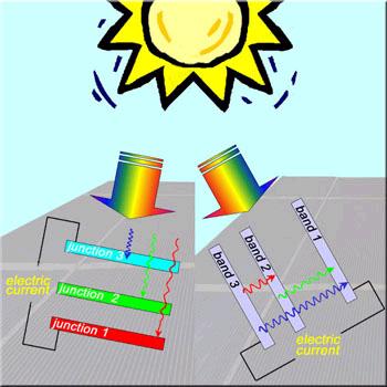
The difference between the material's valence band
and the lower of the split bands forms one band gap. In ZnMnTe incorporating
oxygen impurities (written ZnMnOTe), this first gap absorbs 1.8 eV photons.
The difference between the two split bands is a
second band gap; in ZnMnOTe, this gap absorbs 0.7 eV photons. Finally,
the difference between the valence band and the upper conducting band forms
a third band gap; in ZnMnOTe, this gap absorbs 2.6 eV photons.
Together, these three gaps respond to virtually
the entire solar spectrum. The calculated efficiency of a single-junction
solar cell made with this material would be a remarkable 57 percent. But
while the single-junction architecture is elegantly simple, many questions
have to be answered before ZnMnOTe or any of its highly mismatched cousins
prove they can do the job.
Making p-type and n-type versions of the split-band
material does not appear to pose a problem. But the tricky process of ion
implantation followed by pulsed laser melting is no way to manufacture
semiconductors in bulk. And the oxygen-implanted layer must be at least
0.5 micrometer thick if the material is to absorb all the solar photons
falling on itmore than twice the 0.2-micrometer thickness achieved so
far.
Yu admits that forming highly mismatched alloys
is "challenging from a crystal-growth point of view," but there is hope
that crystals can be grown epitaxially. One good sign, he says, is that
Japanese researchers have already grown thick oxygen-doped crystals of
a related material, zinc selenium.
In the meantime, the Berkeley Lab researchers have
teamed with Piotr Becla of MIT to manufacture a single junction of the
material which gives a photovoltaic response. With it they have demonstrated
the kind of three-band semiconductor needed for high-efficiency, single-junction
solar cells.
There are many possible ways of varying the composition
of these alloys to get the desired resultso many that eventual success
seems as highly likely as the alloys are highly mismatched.
Additional information
"Diluted
II-VI oxide semiconductors with multiple band gaps," by Kin Man Yu,
Wladek Walukiewicz, Wei Shan, and Jeff Beeman of Berkeley Lab, Mike Scarpulla
and Oscar Dubon of Berkeley Lab and UC Berkeley, and Piotr Becla of MIT,
appeared in Physical Review Letters, 12 December 2003.
More about indium
gallium nitride for solar cells
More about the
structures of solar cells